Thin metal films deposited on non-wetting substrates (such as oxide ceramics, diamond or silicon) are thermodynamically unstable because of the large areas of energy-costly metal free surface and metal-substrate interface. Therefore, at elevated temperatures enabling some mobility of surface atoms (but still in the solid state of the film) such films break down into the array of isolated metal particles. The process normally begins with the nucleation of a hole in the film (at random defect, or due to accelerated grooving at the triple junctions of grain boundaries). The supercritical holes expand, and the film material rejected by the hole form an elevated ridge. These ridges late break down into isolated islands, finally evolving to the particles exhibiting the equilibrium crystal shape (see Fig.1).
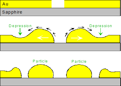
Fig. 1. Schematic of the three stages of solid state dewetting of thin metal (Au) film deposited on ceramic (sapphire) substrate. From the top to the bottom: hole nucleation; hole expansion and formation of elevated ridge; particles formation.
Early theories of solid state dewetting have treated the film material as single crystal, and neglected surface anisotropy of the metal. We have combined the experimental studies of polycrystalline, bi-crystalline and quasi single crystalline thin metal films on sapphire with the theoretical analyses of the film morphology evolution. Sevral milestones of our research are listed below:
- The role of surface anisotropy in solid state dewetting:
The surface energy of most metals is anisotropic, i.e. it exhibits sharp minima (cusps) in the dependencies of the energy of the surface on its orientation. We demonstrated that the solid state dewetting of the film exposing strongly anisotropic surface proceeds without formation of a characteristic depression (as the one shown in Fig. 1b).
L. Klinger, D. Amram, E. Rabkin, Kinetics of retracting solid film edge: the case of high surface anisotropy, Scripta mater. 64 (2011) 962-965
In this work we formulated a one-dimensional kinetic model of solid state dewetting of the thin film with anisotropic surface, and verified its prediction for the quasi-single crystalline Au(Fe) film on sapphire:
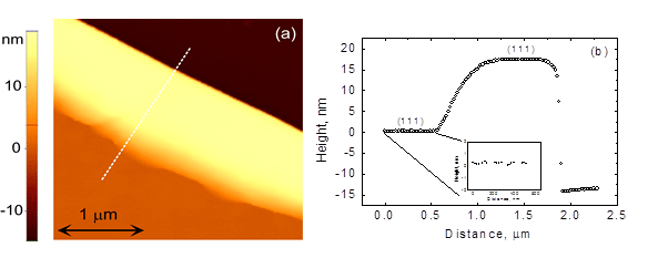
Fig. 2. (a) The atomic force microscopy (AFM) image of the near-hole ridge formed after annealing of 13 nm-thick Au(Fe) film on sapphire at the temperature of 650 C for 7 h. (b) the line topography profile taken along the dashed white line in (a) demonstrating the absence of the depression.
A full three-dimensional model of anisotropic solid state dewetting was developed in the following work:
D. Amram, L. Klinger, E. Rabkin, Anisotropic hole growth during solid-state dewetting of single crystal Au-Fe thin films on sapphire, Acta mater. 60 (2012) 3047-3056
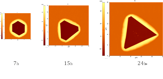
Fig. 3. Temporal evolution of anisotropic hole in the [111]-oriented Au(Fe) film of sapphire. Hexagonal holes evolves into a triangular one due to the difference of {111} and {001} facet diffusivities.
- The role of grain boundary and interface diffusion in solid state dewetting:
Grain boundaries in polycrystalline thin films represent the paths of ultrafast diffusion, on a par with the surface self-diffusion in the film. We proposed a model of solid state dewetting controlled by grain boundary diffusion to explain the formation of hillocks in thin Fe films. The hillocks were formed at some distance from the expanding holes, indicating that the material rejected by the holes somehow “magically” makes it to the hillocks.
O. Kovalenko, J.R. Greer, E. Rabkin, Solid state dewetting of thin iron films on sapphire substrates controlled by grain boundary diffusion, Acta mater. 61 (2013) 3148-3156
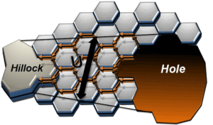
Fig. 4. This is a schematic illustration from our paper above demonstrating how the material gets from the expanding hole to the nearby hillock.
Surface topography of the polycrystalline thin films in the vicinity of expanding holes often exhibits “grainy” appearance, and the corresponding AFM scans identify surface steps formed at the grain boundaries. We interpreted these steps as a sign of interface diffusion of the material from the hole, and concomitant upward drift of the individual grains.
A. Kosinova, L. Klinger, O. Kovalenko, E. Rabkin, The role of grain boundary sliding in solid-state dewetting of thin polycrystalline films, Scripta mater. 82 (2014) 33-36
A. Kosinova, O. Kovalenko, L. Klinger, E. Rabkin, Mechanisms of solid-state dewetting of thin Au films in different annealing atmospheres, Acta mater. 83 (2015) 91-101
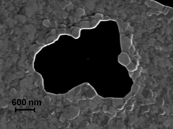
Fig. 5. Terrace-like morphology of polycrystalline Au film in the vicinity of expanding hole.
An interplay of different solid state dewetting mechanisms is described in our work on solid state dewetting of thin Mo films on sapphire:
O. Kovalenko, S. Szabó, L. Klinger, E. Rabkin, Solid state dewetting of polycrystalline Mo film on sapphire, Acta mater. 139 (2017) 51-61
- Chemically-induced solid state dewetting:
In some cases, the reduction of surface and interface energy of the film is not the only driving force of dewetting. In the following work, we deposited thin Au film on the array of the Au-Ag alloy nanoparticles produced by previous solid state dewetting of the Au-Ag bilayer. The alloy particles acted as “magnets” attracting the Au atoms from the Au film, mainly from the triple junctions of the grain boundaries. This resulted in a “Swiss cheese” morphology of the Au film under the conditions at which the same film deposited on bare sapphire substrate preserved its stability:
N. Gazit, L. Klinger, E. Rabkin, Chemically-induced solid-state dewetting of thin Au films, Acta mater. 129 (2017) 300-311
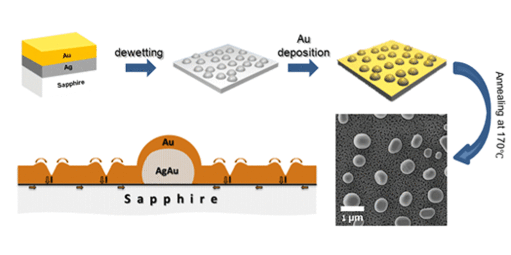
Fig. 6. Graphical abstract of the work on chemically-induced solid state dewetting.